HOME
Nanoscale imaging of dopant nanostructures in silicon-based devices
When fabricating integrated circuits and different types of silicon-based devices, researchers need to position dopant nanostructures in specific ways with high levels of precision. However, arranging these structures at the nanometer scale can be challenging, as their small size makes them difficult to observe and closely examine. Incorrectly tampering with them can have detrimental effects, which can potentially compromise a device's overall functioning and security.
With this in mind, researchers at Johannes Kepler University (JKU), Keysight Technologies Labs, University College London (UCL), and IBM Research have recently set out to develop a nanoscale imaging technique that can be used to observe dopant nanostructures in silicon-based devices with high precision. The method they developed, presented in a paper published in Nature Electronics, is the result of several years of research, following a joint Marie Curie- EU project that kicked-off in 2016.
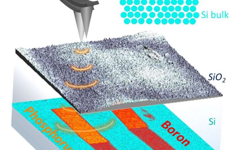
"At JKU and Keysight Technologies Labs I was working on the development of new nanoscale characterization techniques that can look at nanoscale electrical properties of small features below a material's surface," Georg Gramse, one of the researchers who carried out the study, told Phys.org. "The big question for us was: how small can we go or how deep into the surface can we look and still see dopants or other conducting features? The question from our collegues at London Center for Nanotechnology (LCN) and IBM that joined the team a bit later was exactly the opposite: Where are our dopant structures? Are they where they should be, and are they activated and conducting?"
The researchers at JKU and Keysight Technologies Labs developed methods that can create nano-patterns of atomically thin n-type (phosphorus) an p-type (boron) dopant layers in silicon, as well as their resulting p-n junctions. This was done in close collaboration with nanotechnology experts at UCL and IBM.
News Source